Advanced Ceramics | Electronic Packaging | Thermal Management
What is a ceramic substrate?
A ceramic substrate is an electrically insulating ceramic base that supports electronic components and carries patterned metal conductors. In power electronics and advanced packaging, it combines chip support, electrical interconnection, heat transfer, and mechanical stability within one engineered component.
1. What Is a Ceramic Substrate?
In electronic packaging, a ceramic substrate consists of a ceramic base material, such as alumina (Al₂O₃), aluminum nitride (AlN), silicon nitride (Si₃N₄), or beryllium oxide (BeO), together with metal layers that form conductive circuits. Unlike a simple insulating ceramic plate, therefore, a completed ceramic substrate integrates an insulating body with a designed electrical and thermal interface.
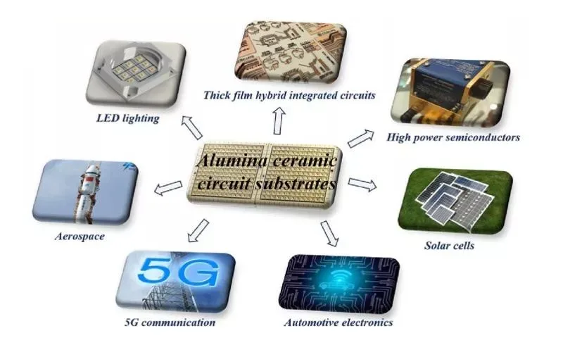
More specifically, the ceramic body separates electrically conductive regions while helping transfer heat from a semiconductor device toward a cooler, heat sink, or cooling structure. Consequently, engineers use ceramic substrates in power semiconductor modules, high-power LEDs, radio-frequency systems, electric vehicles, renewable-energy converters, and other applications that demand reliable electrical insulation and effective heat management.
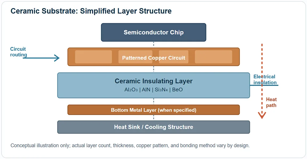
Figure 1. A ceramic substrate integrates a patterned conductor with a ceramic insulating base, while the complete assembly provides paths for both current and heat.
The Four Core Functions of a Ceramic Substrate
Chip Support
First, the substrate provides a stable base for mounting semiconductor dies and other electronic components.
Electrical Interconnection
Next, patterned metal traces create designed electrical paths between components and external terminals.
Heat Transfer
Meanwhile, the ceramic body and metal layers transfer heat toward the cooling system.
Mechanical Stability
Finally, the substrate supports the assembly under mounting loads, thermal cycling, and operating stress.
Taken together, these functions allow a ceramic substrate to support high power density, electrical isolation, and reliable operation in environments that challenge many conventional circuit-board materials.
2. Four Main Ceramic Substrate Materials at a Glance
For material selection, engineers usually balance thermal conductivity against mechanical strength, fracture toughness, thermal expansion, dielectric properties, processability, and cost. The following reference table summarizes the four material families described in the supplied technical document.
| Property | Alumina (Al₂O₃) | Aluminum Nitride (AlN) | Silicon Nitride (Si₃N₄) | Beryllium Oxide (BeO) |
|---|---|---|---|---|
| Thermal conductivity (W/(m·K)) |
15-30 | 170-230 | 60-90 | 200-250 |
| CTE (×10⁻⁶/K) | 6.5-7.5 | 3.5-4.5 | 2.6-3.3 | Approximately 7.5 |
| Flexural strength (MPa) | Approximately 400 | Approximately 350 | 800-1,000 | Approximately 250 |
| Fracture toughness (MPa·m1/2) | Approximately 3 | Approximately 2.7 | 6-7 | Approximately 3.3 |
| Dielectric constant at 1 MHz | Approximately 9.7 | Approximately 8.9 | Approximately 9 | Approximately 6.7 |
| Relative cost in source | Low; reference baseline | Medium-high; about 2-4× alumina | High | Moderate, with significant safety constraints |
| General positioning | Cost-effective, mature mainstream option | High-conductivity option | High-reliability, high-toughness option | Specialized high-conductivity insulating option |
Data note: The table reproduces the approximate figures supplied in substrate.docx. Actual values vary with material grade, purity, density, manufacturing route, test method, and temperature. In particular, buyers should verify the exact substrate grade and test conditions before using these values in a design specification.
Quick Selection Summary
For low cost and mature processing: Alumina (Al₂O₃) provides a practical starting point for many standard electronic substrates.
For heat dissipation: Aluminum nitride (AlN) offers substantially higher thermal conductivity than alumina.
For thermal cycling and mechanical reliability: Silicon nitride (Si₃N₄) stands out for its flexural strength and fracture toughness.
For specialized applications with strict safety controls: Beryllium oxide (BeO) combines high conductivity with electrical insulation, although occupational-health considerations may restrict its use.
3. Alumina (Al₂O₃) Ceramic Substrate: Cost-Effective and Well Established
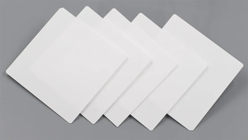
As a mainstream ceramic substrate material, alumina combines mature manufacturing processes with broad industrial availability and relatively low material cost. According to the supplied reference, alumina accounts for approximately 60% of the market, although the actual share depends on the market segment, region, and measurement period.
3.1 Thermal and Mechanical Characteristics
Typically, alumina provides thermal conductivity in the approximate range of 15-30 W/(m·K), which is substantially lower than the values listed for AlN and BeO. Nevertheless, its combination of electrical insulation, useful mechanical strength, mature supply chains, and competitive cost makes it suitable for many applications that do not demand extreme heat dissipation.
In addition, the reference gives an approximate CTE of 6.5-7.5 × 10⁻⁶/K and flexural strength around 400 MPa. Consequently, designers can consider alumina for many general electronic packages, although they must still assess thermal expansion mismatch and mechanical stresses across the complete assembly.
3.2 Manufacturing and Applications
Because manufacturers can use established ceramic processing and metallization routes, alumina supports a broad range of cost-sensitive components. For example, engineers use it in thick-film circuits, chip components, LED packages, insulating plates, and low-to-medium-power electronic assemblies.
Therefore, alumina often represents the first material to evaluate when a design requires dependable insulation and practical manufacturing economics but does not place heat dissipation above every other consideration.
4. Aluminum Nitride (AlN) Ceramic Substrate: Designed for High Heat Dissipation
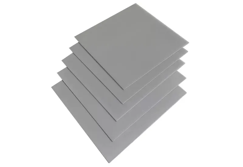
Compared with alumina, aluminum nitride delivers much higher thermal conductivity while maintaining electrical insulation, making it a strong option for power devices and thermally demanding electronic packages. The supplied reference lists a thermal conductivity of approximately 170-230 W/(m·K), together with a CTE of 3.5-4.5 × 10⁻⁶/K.
4.1 Why AlN Supports Thermal Management
In high-power circuits, semiconductor junctions generate heat that must move through the package without creating excessive temperature rise. Accordingly, AlN offers a useful combination of heat transfer and electrical isolation for applications where conventional insulating materials may impose greater thermal resistance.
Furthermore, its relatively low thermal expansion coefficient can help engineers manage dimensional changes in semiconductor assemblies. However, the actual match depends on the particular chip material, joining layer, metal conductor, temperature range, and component geometry rather than on one CTE value alone.
4.2 Processing and Cost Considerations
Despite its thermal advantages, AlN generally costs more than alumina because high-quality raw powders, controlled sintering, and careful process management can increase manufacturing expense. Therefore, the supplied document places AlN at roughly two to four times the cost of alumina as a reference comparison, rather than a universal quotation for every grade or component.
Meanwhile, engineers must confirm density, purity, dielectric behavior, metal-bonding compatibility, and thermal conductivity for the actual substrate grade. For this reason, selecting AlN based solely on a headline conductivity figure may overlook important manufacturing, mechanical, and lifetime requirements.
4.3 Typical Applications
Consequently, AlN is commonly evaluated for high-power LEDs, IGBT modules, power semiconductor packaging, and 5G radio-frequency modules, especially when the thermal design needs more performance than alumina can normally provide.
5. Silicon Nitride (Si₃N₄) Ceramic Substrate: Strength and Thermal-Shock Resistance
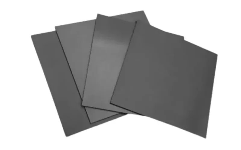
Silicon nitride stands out because it combines useful thermal conductivity with high flexural strength, fracture toughness, and resistance to thermal shock. While its conductivity does not normally reach that of AlN, its mechanical properties can make it attractive for components that experience repeated temperature changes, vibration, or substantial mechanical loading.
5.1 Mechanical Performance
According to the supplied reference, silicon nitride can provide thermal conductivity of approximately 60-90 W/(m·K), flexural strength of 800-1,000 MPa, and fracture toughness around 6-7 MPa·m1/2. These reference values explain why designers often evaluate Si₃N₄ when a substrate must tolerate thermomechanical stress rather than maximize heat transfer alone.
In particular, fracture toughness describes a material’s resistance to crack propagation, while flexural strength characterizes its resistance to failure under bending stress. Consequently, the combination of both properties can be valuable where thermal gradients or repeated power cycling place stress on the ceramic body and its bonded metal layers.
5.2 Why Si₃N₄ Fits Demanding Power Modules
During operation, power modules can experience rapid temperature fluctuations that create expansion and contraction across the ceramic, copper, and semiconductor layers. Therefore, silicon nitride’s toughness and thermal-shock resistance can help support demanding applications, provided that the complete substrate assembly also meets its bonding, fatigue, and thermal requirements.
For this reason, engineers frequently consider Si₃N₄ substrates for automotive SiC power modules, railway traction systems, and aerospace electronics that require high reliability. In such designs, the aim is not simply to maximize the substrate’s thermal conductivity but to preserve the integrity of the entire power module throughout its service life.
5.3 Cost and Design Trade-Offs
Nevertheless, silicon nitride typically carries a higher cost than alumina, and its conductivity remains below the reference range for AlN. Accordingly, engineers should select it when the application justifies its mechanical and reliability advantages rather than treating it as a universal replacement for other ceramic materials.
6. Beryllium Oxide (BeO) Ceramic Substrate: High Conductivity with Important Safety Constraints
Beryllium oxide offers high thermal conductivity alongside electrical insulation, and the supplied reference lists a typical range of approximately 200-250 W/(m·K). As a result, BeO can serve specialized applications where efficient heat transfer and electrical isolation must coexist in a compact ceramic component.

6.1 Thermal and Electrical Characteristics
Relative to alumina, BeO can transfer heat much more effectively, while its listed dielectric constant of approximately 6.7 at 1 MHz differs from those of the other three materials. Accordingly, high-frequency and specialized electronic designs may consider its combination of thermal and dielectric characteristics when other requirements also fit.
However, BeO’s comparatively lower reference flexural strength of about 250 MPa means that engineers must review the component’s mechanical requirements alongside its thermal performance. Similarly, its approximate CTE of 7.5 × 10⁻⁶/K calls for attention to thermal expansion compatibility with adjoining materials.
6.2 Occupational Health and Application Restrictions
Despite its technical advantages, beryllium-containing dust presents a serious occupational-health hazard, particularly during powder handling, machining, grinding, and finishing. Therefore, manufacturers must implement appropriate exposure controls, follow applicable regulations, and review safety documentation before processing BeO components.
Because these safety requirements can complicate manufacturing and maintenance, BeO generally suits specialized applications rather than serving as the default choice for ordinary electronic packaging. Consequently, the material’s technical value must justify the associated workplace controls and compliance burden.
Selection note: BeO should not be chosen on thermal conductivity alone. Instead, designers must assess whether its particular electrical and thermal properties justify the required exposure controls and whether a suitable alternative can satisfy the same performance targets.
7. Ceramic Substrate Metallization: Turning a Ceramic Plate into a Circuit
Although the ceramic body provides electrical insulation and mechanical support, manufacturers must create metal conductor patterns before it can function as an electronic circuit substrate. Accordingly, metallization joins a ceramic base to conductive layers such as copper, silver, or gold, with the selected method affecting conductor thickness, line resolution, bonding strength, manufacturing cost, and thermal-cycle performance.
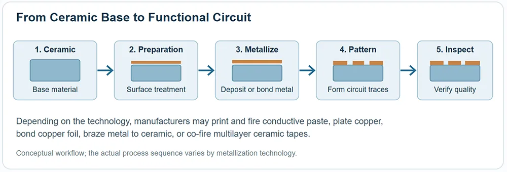
Figure 2. Metallization creates conductive patterns on the ceramic substrate, while the specific bonding and patterning route determines much of the final circuit performance.
7.1 Thick-Film Metallization
In the thick-film route, manufacturers screen-print silver, gold, or copper conductive paste onto the ceramic surface and then fire the deposited material. The supplied reference gives a typical firing temperature of around 850°C and line-width precision of approximately ±50 μm, making this route suitable for cost-sensitive circuits and some medium- or low-power applications.
Therefore, thick-film metallization is worth considering when manufacturing economics and a mature process matter more than the finest conductor geometry.
7.2 DPC: Direct Plated Copper
Direct Plated Copper (DPC) uses a thin seed layer, commonly formed through a deposition process, followed by photolithography, copper electroplating, and pattern definition. According to the supplied document, DPC can achieve conductor feature dimensions around 20 μm, giving it an advantage in fine-pitch circuit layouts.
Consequently, engineers often evaluate DPC for high-density interconnections, LED packages, and selected high-frequency or low-current applications where fine conductor geometry provides an important design benefit.
7.3 DBC: Direct Bonded Copper
Direct Bonded Copper (DBC) joins copper foil to a ceramic substrate through a copper-oxygen eutectic bonding mechanism, with the supplied reference identifying a process range of approximately 1,065-1,085°C. This technology can produce relatively thick copper layers that carry substantial current, making it a longstanding option for medium- and high-power electronic modules.
Nevertheless, designers should examine copper thickness, circuit geometry, ceramic type, bonding quality, and temperature cycling when assessing DBC for a particular module.
7.4 AMB: Active Metal Brazing
Active Metal Brazing (AMB) uses an active brazing alloy containing elements such as titanium to join metal conductors to ceramic. Because this method can form a strong ceramic-to-metal bond, engineers frequently consider AMB for applications that experience demanding thermal cycling and mechanical loads.
In particular, the supplied reference highlights the combination of silicon nitride ceramic and AMB for automotive SiC power modules, where mechanical reliability and thermal-cycle durability play important roles.
7.5 LTCC and HTCC: Multilayer Co-Fired Ceramics
Low-Temperature Co-Fired Ceramic (LTCC) and High-Temperature Co-Fired Ceramic (HTCC) technologies form multilayer structures by stacking ceramic green tapes containing designed conductor patterns and then co-firing the assembly. The supplied document cites approximate processing temperatures around 900°C for LTCC and up to about 1,600°C for HTCC, although actual firing schedules depend on the material system.
As a result, these methods support multilayer routing, integrated passive components, compact three-dimensional packaging, and selected RF front-end systems, including applications operating in the 5G and millimeter-wave domains.
8. How to Choose a Ceramic Substrate Material
When selecting a ceramic substrate, engineers should start with operating requirements instead of choosing the material with the highest thermal conductivity by default. In practice, substrate performance depends on the ceramic grade, metal bonding method, circuit layout, assembly design, temperature range, and expected operating life.
Choose Al₂O₃ When Cost Matters
For general electronic substrates, thick-film circuits, and many LED applications, alumina provides a mature and relatively economical baseline.
Choose AlN When Heat Transfer Leads
For power electronics and high-power packages, AlN is a strong candidate when high thermal conductivity and electrical insulation are both essential.
Choose Si₃N₄ When Reliability Leads
For thermal cycling, shock loading, and high-reliability power modules, silicon nitride offers a valuable combination of toughness and strength.
Evaluate BeO Only for Qualified Needs
For specialized designs, BeO can deliver high thermal conductivity, but the project must account for its occupational-health controls and compliance requirements.
Technical Checklist for Substrate Specification
- First, define the maximum heat load, target junction temperature, and complete thermal path from the semiconductor die to the cooling system.
- Next, confirm electrical insulation, dielectric strength, dielectric constant, and conductor design requirements.
- Additionally, compare the substrate CTE with the semiconductor, copper layer, bonding material, and adjoining package components.
- Meanwhile, verify flexural strength, fracture toughness, thermal-shock resistance, and the expected temperature-cycling profile.
- Furthermore, choose the metallization technology based on copper thickness, line-width requirements, current load, and bonding reliability.
- Finally, compare total component cost, process capability, supplier qualification, inspection requirements, and occupational safety constraints.
9. Where Are Ceramic Substrates Used?
Across the electronics industry, ceramic substrates support applications that require a combination of electrical insulation, heat dissipation, mechanical stability, and packaging reliability. The specific ceramic and metallization route depend on the device’s power level, operating environment, and required service life.
Power Semiconductor Modules
In IGBT, SiC, and MOSFET modules, the ceramic substrate separates electrical regions while helping transfer heat away from semiconductor devices. Accordingly, AlN and Si₃N₄ are important candidates for demanding power electronics, while DBC and AMB provide alternative copper-to-ceramic bonding approaches for different design priorities.
LED and High-Power Lighting
Because LEDs generate heat at compact semiconductor junctions, an appropriate substrate can improve heat transfer and support stable operation. Therefore, engineers may use alumina for cost-sensitive packages or evaluate AlN when greater thermal performance is required.
RF Modules and High-Frequency Electronics
In RF and high-frequency systems, dielectric properties, conductor geometry, circuit loss, and thermal performance all influence the package design. Consequently, material selection and metallization resolution become important for 5G infrastructure, radar, microwave modules, and related electronic assemblies.
Electric Vehicles and Renewable Energy
Electric-vehicle traction inverters, charging systems, and photovoltaic converters use power electronics that experience electrical and thermal stress. For this reason, ceramic substrates with appropriate heat transfer, conductor bonding, and thermal-cycle durability can help support reliable power conversion.
Aerospace, Railway, and High-Reliability Systems
Meanwhile, railway traction equipment, aerospace electronics, and other high-reliability systems may require substrates that balance thermal performance with resistance to vibration, temperature changes, and mechanical stress. In these applications, engineers must validate the entire package rather than rely on a single material property.
10. Frequently Asked Questions About Ceramic Substrates
What is the main purpose of a ceramic substrate?
Primarily, a ceramic substrate supports semiconductor components, provides electrical insulation, routes current through patterned metal conductors, and transfers heat toward the cooling structure. Consequently, it forms a key part of many power-electronic and high-performance electronic packages.
Which ceramic substrate material has the highest thermal conductivity?
Among the four materials compared in this article, BeO and AlN have the highest conductivity ranges in the supplied reference, with BeO listed at approximately 200-250 W/(m·K) and AlN at 170-230 W/(m·K). However, actual performance depends on the selected grade and processing conditions, while BeO also requires strict exposure controls.
Why do engineers choose silicon nitride instead of aluminum nitride?
Although AlN generally offers higher thermal conductivity, Si₃N₄ provides higher flexural strength and fracture toughness in the comparison presented here. Therefore, silicon nitride can be more attractive when a power module must withstand severe thermal cycling and mechanical stress.
What is the difference between a ceramic substrate and a ceramic plate?
Generally, a bare ceramic plate serves as an insulating or structural component, whereas a ceramic substrate for electronic packaging includes designed metal conductors or other metallized features. Thus, metallization and circuit design distinguish a functional ceramic circuit substrate from a plain ceramic plate.
What are DBC, DPC, and AMB ceramic substrates?
Specifically, DBC uses a copper-oxygen bonding mechanism to join copper foil to ceramic, DPC forms conductor patterns through deposition, plating, and patterning, while AMB uses an active brazing alloy to join metal and ceramic. Consequently, each route provides a different balance of conductor thickness, circuit resolution, bonding performance, and process requirements.
Is alumina suitable for power electronics?
Yes, alumina can suit many electronic and lower-to-medium-power applications when its thermal performance meets the system requirements. Nevertheless, engineers may prefer AlN or Si₃N₄ for more demanding thermal or thermomechanical conditions.
Why does ceramic substrate material selection affect reliability?
Because thermal conductivity, CTE, strength, toughness, and metal-bonding behavior jointly influence operating temperature and thermomechanical stress, material choice affects the complete package. Accordingly, engineers should evaluate the ceramic, conductor layers, bonding interface, chip, and cooling structure as one integrated system.
Conclusion: Ceramic Substrates Balance Heat, Insulation, and Reliability
Ultimately, a ceramic substrate is more than an insulating plate; it is an engineered circuit base that connects electrical routing, thermal management, mechanical support, and semiconductor packaging. Among the four main materials, alumina offers a cost-effective and mature solution, AlN prioritizes high thermal conductivity, Si₃N₄ emphasizes mechanical reliability and thermal-shock resistance, and BeO provides high conductivity for specialized applications with strict safety requirements.
Meanwhile, metallization technology determines how effectively the ceramic body integrates with copper conductors and the surrounding electronic assembly. Therefore, designers should assess the ceramic grade and the DBC, DPC, AMB, thick-film, or co-fired process as a combined design decision rather than selecting either in isolation.
For practical engineering, the best ceramic substrate is the one that meets the application’s verified thermal, electrical, mechanical, manufacturing, cost, and reliability requirements. Accordingly, engineers should use grade-specific supplier data and assembly-level validation to turn material properties into dependable product performance.