Materials Engineering · Semiconductor Manufacturing · Power Electronics
How Silicon Nitride Ceramics Permeate the Entire Semiconductor Equipment Supply Chain?
From high-quality Si₃N₄ powder to precision ceramic parts and copper-bonded power substrates, silicon nitride connects materials science with process equipment, advanced packaging, and reliable power conversion.
At a Glance
To understand silicon nitride’s role, first distinguish two connected but different areas of the semiconductor ecosystem: wafer-fabrication equipment and power-semiconductor packaging. Within wafer-processing tools, ceramic components support precise handling, thermal stability, wear resistance, and contamination control; meanwhile, in power modules, a silicon nitride ceramic substrate provides electrical insulation and a mechanically robust thermal path for devices such as silicon carbide (SiC) MOSFETs. For this reason, Si₃N₄ is not a universal material for every machine or chip package, but it is a strategically useful option where strength, thermal cycling, and insulation must work together.
Across practical manufacturing, the supply chain begins with powder chemistry and microstructure control, continues through forming, debinding, sintering, grinding, and inspection, and may then add active metal brazing (AMB) to create a copper-clad substrate. Ultimately, application-specific qualification determines whether a component performs reliably inside a semiconductor tool or a high-power module.
1. Why Silicon Nitride Matters in Semiconductor Systems
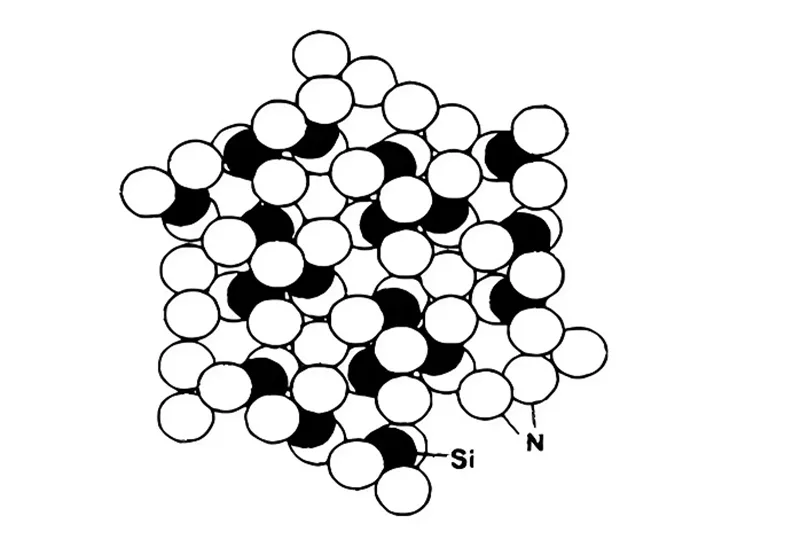
Unlike a metallic structural part, silicon nitride (Si₃N₄) is a covalently bonded engineering ceramic that combines high mechanical strength, useful fracture toughness for a ceramic, low thermal expansion, wear resistance, and electrical insulation. Moreover, its performance depends on crystal phase, grain morphology, porosity, impurities, sintering aids, and final machining quality; therefore, material name alone never guarantees an application-ready result.
Regarding power electronics, engineers often evaluate Si₃N₄ as the insulating layer in an AMB copper-clad substrate. Copper traces carry current, the ceramic electrically isolates those circuits from the baseplate or cooler, and the substrate conducts heat away from the semiconductor dies. Under demanding automotive or industrial duty cycles, the combination of ceramic toughness and thermal-mechanical durability can be more valuable than maximizing thermal conductivity alone.
Conversely, silicon nitride can also serve as a precision ceramic in selected semiconductor-equipment mechanisms, including application-specific wafer-handling or positioning components. Even so, actual tool designs may instead specify alumina, aluminum nitride, silicon carbide, quartz, or other materials according to plasma exposure, process chemistry, temperature, purity, electrical behavior, and particle-control requirements. Hence, supplier selection should start with the component function and process environment rather than with a blanket assumption that Si₃N₄ is always the preferred ceramic.
Effective from January 1, 2026, China’s national standard GB/T 45767-2025, titled Silicon Nitride Ceramic Substrates, took effect on January 1, 2026. This standard demonstrates the growing importance of substrate-level specification, although a supplier and customer still need to agree on the relevant grade, dimensions, copper-bonding process, and application tests. Open the official standard record.
2. Si₃N₄ Powder Production: The First Link in the Chain
Before manufacturers can press or cast a reliable ceramic substrate, they need powder with controlled phase composition, particle-size distribution, morphology, oxygen content, metallic impurities, and surface chemistry. Furthermore, powder batches need consistent flow and packing behavior because variations at this stage can propagate into uneven shrinkage, warpage, pores, and local weaknesses after sintering.
2.1 Principal synthesis routes
One established route is direct nitridation, in which silicon powder reacts with nitrogen at elevated temperature to form silicon nitride. That route can offer a relatively direct raw-material pathway, although reaction heat, nitrogen transport, powder agglomeration, and the residual unreacted silicon content require careful control. Meanwhile, the carbothermal reduction and nitridation route reacts a silica-containing precursor with carbon under nitrogen; manufacturers then remove residual carbon and refine the powder to meet downstream requirements.
Beyond these routes, chemical vapor deposition or precursor-conversion approaches can serve specialized needs where chemistry, particle morphology, or purity justifies their additional process complexity. Ultimately, no single synthesis method is best for every grade: the target phase, cost structure, scale, impurity limits, and ceramic application all influence the appropriate route. Published technical reviews on Si₃N₄ powder preparation identifies fine particle size, a narrow size distribution, high α-phase content, and low impurity levels as important targets for high-performance powder. Explore the powder preparation review.
SVG Process Diagram 1 – Silicon Nitride Powder Supply Route
This schematic summarizes two mainstream powder-synthesis paths and the shared finishing and quality-control stages.
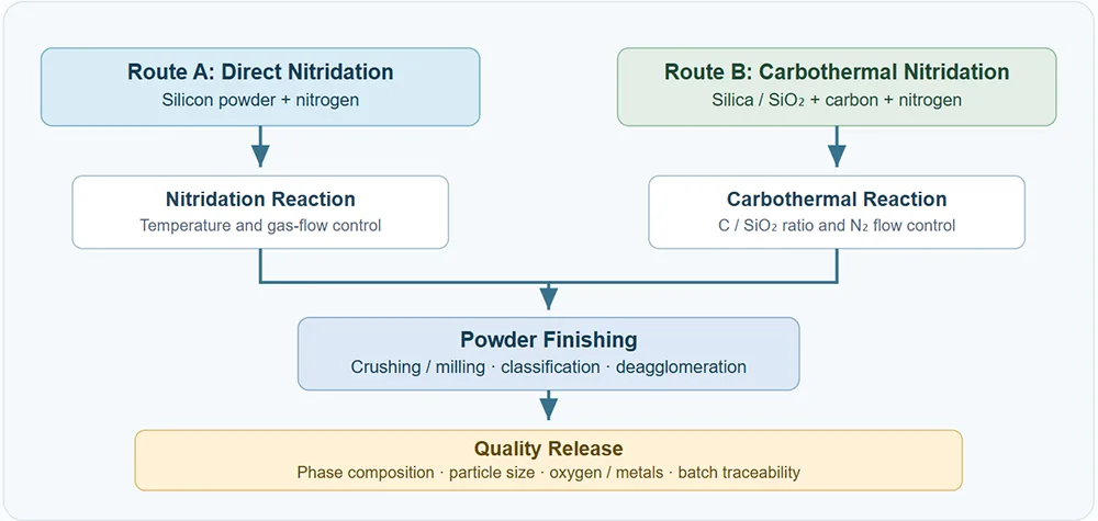
Note: The diagram is a high-level process map. Exact reaction conditions, post-treatment steps, and acceptance limits depend on the powder grade and supplier route.
2.2 Why powder consistency affects the final substrate
During ceramic processing, α-Si₃N₄ commonly transforms toward β-Si₃N₄ and develops elongated grains under suitable liquid-phase sintering conditions. Such a microstructure can help improve crack resistance through grain bridging and crack deflection, but the final result also depends on additives, firing atmosphere, temperature profile, and cooling schedule. Therefore, powder suppliers should report phase content and impurity data using agreed methods rather than relying only on a generic “high-purity” label.
Beyond that, powder quality affects the economics of later stages. Agglomerates can create local density gradients; excessive oxygen can alter grain-boundary phases; and poor particle packing can increase shrinkage variation. Accordingly, manufacturers should connect incoming powder inspection to substrate yield, dimensional stability, thermal conductivity, and strength data from finished parts.
3. From Ceramic Powder to a Silicon Nitride AMB Substrate
A powder batch becomes an insulating ceramic substrate only after several controlled process stages. First, manufacturers mix Si₃N₄ powder with selected sintering aids and a forming system; next, they shape the mixture through tape casting, pressing, or another validated method. Next, binder removal and sintering establish the ceramic’s density and microstructure, while grinding and lapping bring the substrate to its required thickness, flatness, and surface condition.
Following ceramic manufacture, an AMB process bonds copper to one or both sides of the Si₃N₄ plate using an active braze system. A Cu–Si₃N₄–Cu structure combines conductive copper circuits with an electrically insulating ceramic core. Unlike AMB, direct-bonded copper (DBC) generally relies on a different copper-to-ceramic bonding mechanism; engineers select AMB or DBC based on the ceramic, circuit design, copper thickness, required bond integrity, thermal cycling profile, and overall cost.
SVG Process Diagram 2 – Si₃N₄ Ceramic Substrate and AMB Production
The first lane builds the ceramic body; the second lane creates the copper-clad substrate and verifies its reliability.
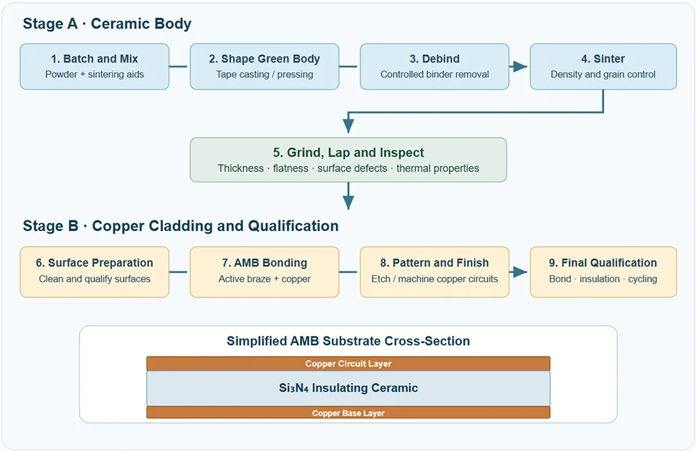
Illustration only: actual layer thicknesses, braze chemistry, copper pattern geometry, and production conditions vary by design and supplier.
3.1 Why AMB is used in demanding power modules
For high-power packaging, active metal brazing can create a robust bond between copper and a ceramic that does not bond readily to copper by ordinary soldering. Such a substrate must carry current, electrically isolate the semiconductor, and transfer heat from the die to a cooling structure. Within an SiC module, that thermal path matters because high switching performance does not remove the need to manage junction temperature and temperature gradients.
Still, a high-strength ceramic does not eliminate reliability risks. Published research on Si₃N₄ substrates has documented cracking associated with improper sintering and nonuniform ingredient mixing, while AMB reliability studies have observed edge-side cracking after severe thermal-shock cycling. Therefore, powder uniformity, firing schedules, plate flatness, copper layout, braze-interface quality, and edge geometry all contribute to long-term reliability. Examine a substrate-cracking failure analysis and review thermal-shock findings for AMB substrates.
4. Applications Across the Semiconductor Supply Chain
4.1 Power-module substrates for SiC devices
In electric vehicles, fast chargers, industrial drives, renewable-energy inverters, and other power-conversion systems, SiC MOSFETs and diodes can support high-voltage and high-frequency switching. Even so, device performance depends on the complete package, including die attach, interconnects, ceramic substrate, baseplate or cooler, encapsulation, and the cooling system. Accordingly, a Si₃N₄ AMB substrate does not independently create higher vehicle range or faster charging; rather, it can help a well-designed module manage heat and mechanical stress reliably.
During operation, current flows through the copper circuit while heat moves from the semiconductor die across its attach layer and copper, through the ceramic, and toward the heat sink. Meanwhile, the ceramic blocks electrical current from passing to the heat sink or chassis. That dual role makes the substrate a functional and reliability-critical part of the package, not simply a passive plate.
4.2 Ceramic parts in wafer-handling and positioning systems
Within wafer-fabrication equipment, ceramic end effectors, arms, support pads, pins, guides, and fixtures can help position or transport fragile wafers and process carriers. Depending on the design, Si₃N₄ may offer a useful balance of mechanical strength, wear behavior, thermal stability, and electrical properties. Still, buyers should not infer that all these components use Si₃N₄; tool builders routinely compare several ceramics and select the material after considering the chemistry and contamination budget of the process chamber.
As an example, a wafer-handling arm needs geometric stability, low particle generation, edge quality, and a controlled contact surface. Conversely, a component exposed to plasma or highly reactive gas may need a different surface chemistry or a ceramic grade selected for exceptional purity. Therefore, the product drawing should define contact zones, datum surfaces, surface finish, dimensional tolerance, cleaning requirements, and acceptance criteria before the supplier chooses its final process.
Semiconductor equipment suppliers describe ceramic handling products across multiple material families, including alumina, zirconia, silicon nitride, and silicon carbide. Such evidence illustrates the breadth of ceramic engineering in the tool chain, but the final material remains application-specific. Review examples of ceramic components for wafer processing.
4.3 Precision mechanisms and supporting components
Beyond direct wafer contact, silicon nitride ceramics can support selected precision mechanisms where wear resistance, low density, dimensional stability, or electrical insulation add value. Even so, the designer must consider brittle fracture, edge chipping, fastener loads, local stress concentration, and the difficulty of machining dense ceramics. Therefore, generous radii, suitable contact geometry, controlled clamping, and well-defined tolerances can matter as much as the headline material properties.
4.4 The connected supply chain
Viewed end to end, the silicon nitride ecosystem links powder synthesis, powder processing, ceramic forming, debinding, sintering, precision finishing, inspection, substrate metallization, module assembly, and end-use qualification. Critically, each handoff needs traceability because a defect that starts as a chemistry or mixing variation may later appear as a substrate crack, an electrical insulation failure, a thermal-resistance shift, or a module reliability issue. In turn, cross-stage data sharing can be as important as investment in any single processing machine.
5. Qualification: What Engineers and Buyers Should Verify
For powder sourcing, request batch-level records for chemical purity, oxygen and metallic impurities, α/β phase composition, particle-size distribution, specific surface area when relevant, and agglomeration behavior. Also establish sample-retention and change-notification rules so that a new synthesis lot, milling condition, or raw-material source does not silently alter a qualified grade.
When specifying ceramic substrates, define thickness, flatness, dimensional tolerance, surface roughness, density or porosity limits, thermal conductivity at a stated temperature, flexural strength, fracture toughness, and dielectric properties. Furthermore, evaluate the copper side: copper thickness and pattern, bond or peel strength, edge condition, voids, delamination, insulation resistance, and partial-discharge behavior may all matter to the final module. One conductivity figure cannot substitute for this broader acceptance plan.
For assembled modules, validation can include thermal cycling, power cycling, high-temperature reverse-bias or other electrical stress testing as appropriate, humidity-bias testing, vibration, shock, and destructive failure analysis. For qualification, test severity and acceptance thresholds should reflect the application standard and the customer’s mission profile; one accelerated test result does not automatically predict every field lifetime.
| Supply-chain stage | Critical controls | Common risk if control slips |
|---|---|---|
| Powder synthesis | Purity, phase, particle size, oxygen, batch traceability | Variable sintering, defects, inconsistent properties |
| Forming and sintering | Homogeneous mixing, green density, atmosphere and thermal cycle | Porosity, warpage, local weakness or cracks |
| Grinding and finishing | Thickness, flatness, edge condition, surface damage | Stress concentrators and assembly mismatch |
| AMB copper bonding | Braze interface, copper layout, bond strength, voids | Delamination, edge cracks, increased thermal resistance |
| End-use validation | Thermal / power cycling, dielectric tests, cleanliness | Premature field failure or contamination |
5.1 A practical sourcing checklist
- First, provide a drawing, process environment, operating temperature range, electrical isolation target, and expected thermal or power-cycling profile.
- Next, ask whether the proposal concerns a bare Si₃N₄ ceramic, a metallized or AMB substrate, or a finished precision equipment component.
- Afterward, request material certificates, agreed inspection methods, sample data, traceability, and an explicit change-control process.
- Finally, qualify the component inside a representative assembly whenever possible, since ceramic, copper, joining layers, cooling hardware, and packaging interact during service.
6. Frequently Asked Questions
What does silicon nitride do in a power semiconductor module?
Inside an AMB substrate, Si₃N₄ forms an electrically insulating ceramic core that supports copper conductors and transfers heat away from semiconductor dies. In addition, its strength and toughness can help the substrate endure mechanical and thermal loads, although the entire module design determines final reliability.
Why does powder quality matter so much?
Because particle size, phase composition, oxygen, impurities, and agglomeration affect forming and sintering, powder consistency helps determine final density, microstructure, dimensions, and mechanical properties. Hence, incoming powder inspection should connect directly to finished-part qualification.
Does silicon nitride replace every other ceramic in semiconductor tools?
No. Instead, equipment designers select among Si₃N₄, SiC, Al₂O₃, AlN, quartz, and other materials according to process chemistry, purity, electrical needs, thermal conditions, wear, and cost.
Is a silicon nitride substrate the same as a silicon carbide semiconductor chip?
No. Unlike an SiC chip, a Si₃N₄ substrate is a ceramic packaging component, while an SiC chip is a semiconductor device that performs electrical switching. At package level, the chip and ceramic substrate work together but serve different physical and electrical functions.
Which data should a buyer request before placing an order?
As a baseline, request the material grade, dimensions and tolerances, thermal and mechanical data with test conditions, copper-bonding specifications when applicable, electrical insulation results, defect criteria, traceability, and evidence from tests relevant to the intended application.
Conclusion
Ultimately, silicon nitride’s contribution to the semiconductor supply chain begins long before a component reaches a tool or power module. Consistent powder chemistry supports repeatable sintering, controlled ceramic microstructure enables reliable substrate performance, precision finishing prepares the surface, and qualified copper bonding creates the current-carrying package interface. Even so, selected Si₃N₄ parts can support wafer handling and precision mechanisms when the process environment suits the material. Therefore, the strongest sourcing strategy evaluates the entire chain-from powder traceability to final-system reliability-instead of judging performance from a single material datasheet.
Technical References
- State Administration for Market Regulation, GB/T 45767-2025 Silicon Nitride Ceramic Substrates, effective January 1, 2026. Official standard record.
- “Research advances in preparation technology and quality of silicon nitride powder,” CIESC Journal. Article abstract.
- Chen et al., “Failure analysis on the abnormal cracking of Si₃N₄ ceramic substrates for SiC power modules in new energy vehicles,” Microelectronics Reliability (2024). Article page.
- Kim et al., “Heat-resistant durability of AMB substrates for SiC power devices: AlN and Si₃N₄, which one is thermally strong?” Microelectronics Reliability (2025). Article page.
- JFM, overview of ceramic components for semiconductor wafer processing. Application reference.