
The Imperative for Advanced Ceramics in Wafer Fab
As semiconductor nodes shrink below 3nm and 2nm, the tolerances for particle contamination, thermal fluctuation, and plasma-induced damage approach absolute zero. Traditional materials like aluminum, stainless steel, and standard quartz are no longer viable for critical chamber components and wafer handling systems. Silicon Nitride (Si₃N₄) has emerged as the premier advanced ceramic for semiconductor equipment, offering an unmatched combination of ultra-high purity, exceptional plasma erosion resistance, and superior mechanical toughness. This comprehensive guide details the engineering, application, and customization of Si₃N₄ components that keep modern fabs running at peak yield.
1. Understanding Si₃N₄: Material, Manufacturing, and Specifications
Material Properties for Semiconductor Environments
Semiconductor-grade Silicon Nitride is not a standard structural ceramic; it is a highly engineered material. Its primary advantages in a fab environment include:
- Plasma Erosion Resistance: Si₃N₄ exhibits significantly lower etch rates in fluorine and chlorine-based plasmas compared to Alumina (Al₂O₃) or Yttria (Y₂O₃), drastically reducing particle generation and extending component lifespan.
- Thermal Shock & Stability: With a low coefficient of thermal expansion (CTE ~3.2 × 10⁻⁶/°C) and high thermal conductivity, it withstands the rapid thermal cycling of CVD and etch chambers without micro-cracking.
- Mechanical Toughness: Its unique elongated beta-grain microstructure provides a fracture toughness of 6-8 MPa·m¹/², making it highly resistant to the chipping and breakage that plague brittle ceramics during robotic wafer handling.
- Electrical Insulation: High dielectric strength prevents arcing and electrostatic chuck (ESC) interference in high-voltage plasma environments.
Advanced Manufacturing Processes
Achieving the required density and purity demands rigorous manufacturing protocols:
Powder Synthesis & Forming
High-purity α-Si₃N₄ powder is blended with rare-earth sintering aids. Forming is achieved via Cold Isostatic Pressing (CIP) for large blanks or Ceramic Injection Molding (CIM) for complex, high-volume micro-components.
Gas Pressure Sintering (GPS)
Firing under high nitrogen pressure (up to 10 MPa) at 1900°C prevents the decomposition of Si₃N₄, promoting full densification and the critical α-to-β phase transformation for toughness.
Hot Isostatic Pressing (HIP)
For mission-critical parts, HIP applies 200 MPa of argon pressure at high temperatures, eliminating all residual micro-porosity to achieve >99.99% theoretical density, preventing outgassing in vacuum chambers.
Strict Specification Requirements
Semiconductor OEMs demand exacting specifications for Si₃N₄ components:
| Parameter | Semiconductor Grade Requirement |
|---|---|
| Purity (Metallic Impurities) | < 1 ppm (Fe, Cu, Na, K strictly controlled in ppb) |
| Density | > 3.25 g/cm³ (>99.9% theoretical via HIP) |
| Surface Roughness (Wafer Contact) | Ra < 0.05 μm (Mirror polish to prevent micro-scratching) |
| Dimensional Tolerance | ± 0.002 mm (CNC diamond ground) |
| Porosity | 0% open porosity (Zero outgassing in vacuum) |
2. Critical Applications in Semiconductor Equipment
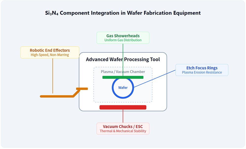
Silicon Nitride is deployed across multiple subsystems within a modern wafer fab, primarily where plasma resistance, mechanical wear, and thermal stability intersect.
Plasma Etch & CVD Chambers
Focus Rings, Showerheads, and Edge Rings. Si₃N₄ resists aggressive fluorine plasmas, maintaining uniform etch profiles and minimizing particle defects that kill die yield.
Wafer Handling & Robotics
End Effectors, Vacuum Chucks, and Forks. Its high stiffness and low weight allow high-speed robotic movement without deflection, while its non-marring surface protects delicate wafers.
Lithography & Inspection
Stage Components and Mirror Mounts. Exceptional dimensional stability and low CTE ensure nanometer-level alignment accuracy during extreme ultraviolet (EUV) lithography.
CMP (Chemical Mechanical Planarization)
Retention Rings and Dressers. Extreme wear resistance against abrasive silica slurries ensures uniform wafer polishing and extends consumable life.
3. How to Customize Si₃N₄ Components for Semiconductor Use
Customizing a ceramic component for a semiconductor tool is a rigorous engineering process. It requires bridging the gap between the OEM’s mechanical design and the physical realities of ceramic manufacturing. The workflow below outlines the critical steps from initial concept to final cleanroom packaging.
The AOFE Custom Si₃N₄ Engineering Workflow
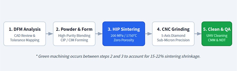
Step 1: Design for Manufacturability (DFM): Semiconductor designs often feature sharp corners or thin walls that induce stress in ceramics. AOFE engineers analyze the CAD model, suggesting radii adjustments and uniform wall thicknesses to prevent cracking during the sintering phase.
Step 2 & 3: Forming and HIP Sintering: After blending ultra-high purity powders, the green body is formed. It is then pre-machined (green machining) to near-net shape. The critical HIP sintering phase follows, applying immense heat and isostatic pressure to achieve the >99.99% density required to prevent outgassing in UHV (Ultra-High Vacuum) environments.
Step 4: Hard Machining & Polishing: Sintered Si₃N₄ is exceptionally hard. We utilize specialized 5-axis CNC machines equipped with diamond grinding wheels to achieve final dimensions. For wafer-contact surfaces, multi-step diamond lapping achieves mirror finishes (Ra < 0.05 μm) to prevent micro-scratches on silicon wafers.
Step 5: Cleanroom Cleaning & QA: The final component undergoes rigorous ultrasonic cleaning in ultrapure water (UPW) and solvents to remove all particulates. It is then packaged in Class 100 cleanroom conditions. QA includes Coordinate Measuring Machine (CMM) verification and Non-Destructive Testing (NDT) to ensure zero subsurface defects.
AOFE: Your Partner in Semiconductor Ceramics
AOFE Advanced Ceramics is a specialized manufacturer dedicated to solving the most complex material challenges in semiconductor fabrication. We understand that a single particle defect can cost thousands of dollars in ruined wafers. Our vertically integrated facility is engineered specifically to produce the ultra-pure, high-precision Si₃N₄ components that leading semiconductor OEMs demand.
The AOFE Advantage for Wafer Fab Equipment
Frequently Asked Questions (FAQ)
Why is Si₃N₄ preferred over Alumina or Quartz in plasma etching?+
Silicon Nitride offers superior resistance to fluorine and chlorine-based plasmas compared to Alumina, significantly reducing particle generation that causes yield loss. Unlike Quartz, Si₃N₄ provides much higher fracture toughness and better thermal shock resistance, preventing catastrophic cracking during the rapid thermal cycling inherent in etch and CVD chambers.
What are the critical purity requirements for Si₃N₄ in wafer fabrication?+
Semiconductor-grade Si₃N₄ must have ultra-low metallic impurities, typically measured in parts per billion (ppb). Elements like Iron (Fe), Copper (Cu), and Sodium (Na) must be strictly controlled to prevent wafer contamination. Additionally, the material must exhibit near-theoretical density (>99.9%) via HIP sintering to eliminate micro-porosity that could harbor contaminants or outgas in vacuum environments.
How does AOFE ensure dimensional accuracy of complex custom parts?+
AOFE utilizes a combination of precision Ceramic Injection Molding (CIM) or Cold Isostatic Pressing (CIP) followed by advanced 5-axis CNC diamond grinding. Because sintered Si₃N₄ is extremely hard (HV 1600+), we use specialized diamond tooling and proprietary lapping processes to achieve ultra-tight tolerances of ±0.002mm and mirror surface finishes (Ra < 0.05 μm) required for wafer contact surfaces.
What is the typical lead time for custom semiconductor-grade Si₃N₄?+
For standard geometries machined from existing HIP-sintered blanks, lead times are typically 3-4 weeks. For highly complex, custom-engineered parts requiring new tooling, specific powder formulations, or extensive CNC profiling and polishing, the lead time ranges from 6 to 10 weeks. AOFE offers expedited prototyping services for critical path semiconductor tool development.
Can Si₃N₄ be used for Electrostatic Chucks (ESC)?+
Yes, while standard Si₃N₄ is an insulator, AOFE can engineer custom Si₃N₄ formulations with tailored electrical resistivity (semi-insulating) specifically for use as the dielectric layer in Johnsen-Rahbek (JR) type Electrostatic Chucks, providing excellent clamping force and thermal transfer in plasma etch tools.
Optimize Your Fab Yield with AOFE Ceramics
Don’t let particle contamination or component failure bottleneck your tool performance. Upload your CAD files today for a comprehensive DFM analysis and a competitive quote on ultra-pure Si₃N₄ components.